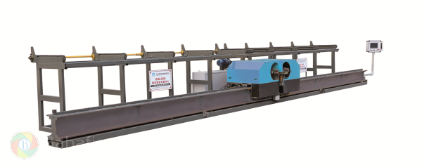
https://xycsteelmachine.com/g2l40a-cnc-center-automatic-rebar-bending-machine/
Automatic rebar bending machines are engineered to simplify steel reinforcement processing with high-speed and accurate bending capabilities. These systems improve construction productivity by reducing manual effort and delivering consistent bending results for various rebar sizes. Built with durable components and advanced automation, they support large-scale construction and infrastructure projects efficiently. Their reliable performance, precision control, and modern technology make them essential equipment for professional steel fabrication operations.
#AutomaticRebarBendingMachine #RebarProcessing #ConstructionEquipment #SteelFabrication #IndustrialMachinery #AutomationTechnology #BuildingProjects
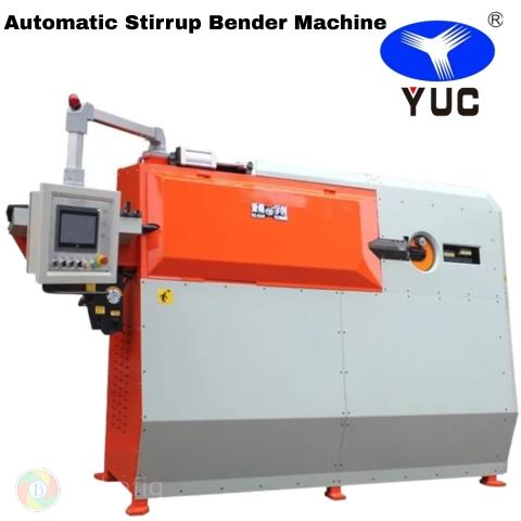
https://xycsteelmachine.com/g2l40a-cnc-center-automatic-rebar-bending-machine/
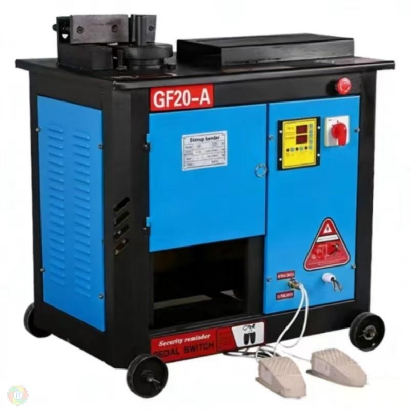
Automatic rebar bending machines are engineered to simplify steel reinforcement processing with high-speed and accurate bending capabilities. These systems improve construction productivity by reducing manual effort and delivering consistent bending results for various rebar sizes. Built with durable components and advanced automation, they support large-scale construction and infrastructure projects efficiently. Their reliable performance, precision control, and modern technology make them essential equipment for professional steel fabrication operations.
#AutomaticRebarBendingMachine #RebarProcessing #ConstructionEquipment #SteelFabrication #IndustrialMachinery #AutomationTechnology #BuildingProjects